Homemade FPGA Miner From Scratch
My most challenging personal project so far is a custom FPGA cryptocurrency miner built from scratch. It isn’t well documented, and there’s too much to go back and fix it up now, but it was too much effort not to write a little something about it. This post is very much a rough draft work in progress but I wanted to get something out there asap to capture at least a little something about the project.

INTRODUCTION:
Recently, I finished creating my own FPGA cryptocurrency miner for the SQRL Acorn Boards.
Due to my interest in cryptocurrency FPGA mining, I have collected a handful of FPGAs that I otherwise would not have. My favorite of the bunch are the Acorn boards. The Acorn was Designed for heterogeneous computing to offload different parts of algorithms that are better suited to FPGAs than to GPUs but leverage the advantages of GPUs as well. Designed to fit in an M.2 Slot and have the bandwidth of PCIe for effective communication with a GPU, more can be read about the hardware from my previous post here.
I also like the Acorns because they are the cheapest of the boards I have, so if I were to break one, it wouldn’t be too hard to swallow.
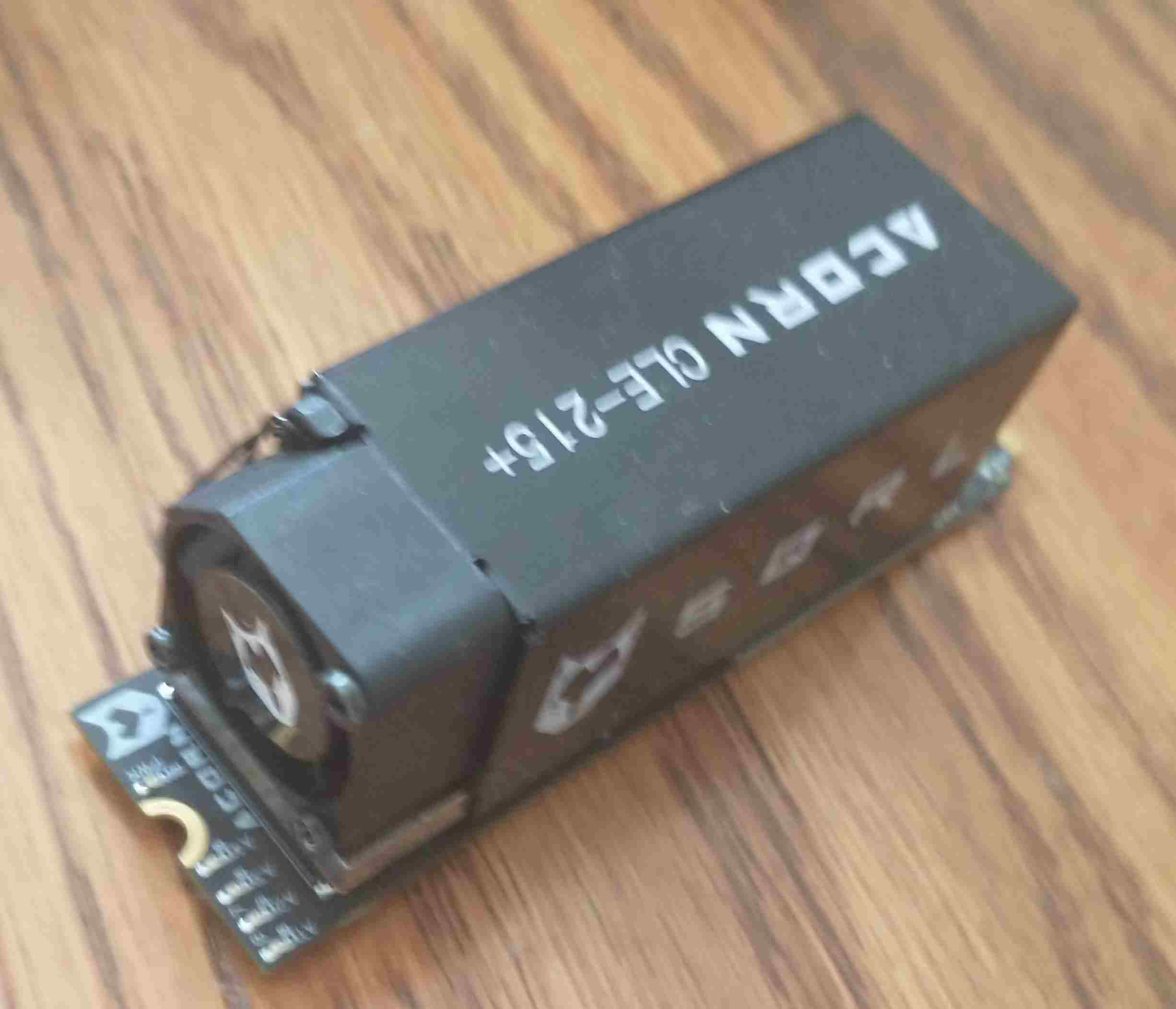
The mighty Acorn.
I wanted to target this platform because these boards never fulfilled their original compute assist intentions, and only the no-longer-existing manufacturer had ever released one useful application for them that only lasted a few months. Everyone’s investments have sat there and collected dust. I was determined to be the first person to put them to work. But had to do so without any support at all.
This project was a huge undertaking. Some of the highlights involved :
- Reading a cryptocurrency codebase in a language I was unfamiliar with to understand the cryptographic hash function involved in mining
- Implementing a hash core in a Hardware Description Language (HDL)
- Writing a UART to AXI-Lite master memory mapped io block in a brand new language (SpinalHDL) to be able to send and receive data to and from the core
- Learning the intricacies of Vivado to get a large design programmable to the FPGA
- Wiring up a UART to USB adapter bridging a PC host and the FPGA and creating a driver on a host computer to communicate to the FPGA
- Integrating that driver into the cryptocurrency node codebase written in another new-to-me language, as mining pools don’t exist
- Getting the cryptocurrency node up and running
- Adding a difficulty checker to report any found hashes
- Coordinating multiple FPGAs at one time
- Discovering and figuring out how to mitigate board design flaws
- And adding safety, connection loss power saving, and clock tuning features to benefit the FPGA effectiveness.
SPINALHDL:
While doing my master’s thesis on High-Level Synthesis (HLS), I came across an interesting Hardware Description Language called SpinalHDL that I immediately grasped the enormous potential of. I think it has enormous potential because it uses modern expressive languages to generate VHDL and Verilog. You can do in 3 simple lines what may take 30 lines the usual way. Most importantly, you can (mostly) understand the generated output and map it back to the SpinalHDL implementation. SpinalHDL is actually just a scala library, which has the benefit that it allows for a really snazzy testing environment, too, including leveraging Verilator for fast simulation. As part of this project, I wanted to get my hands dirty using SpinalHDL for real for the first time.
The first development was to build a UART to AXI-Lite master. AXI is a pretty neat protocol, but learning the ins and outs and building an AXI-Lite master in an unfamiliar language was a decently sized undertaking. It isn’t the cleanest code in the world, but it can be found here.(TODO)
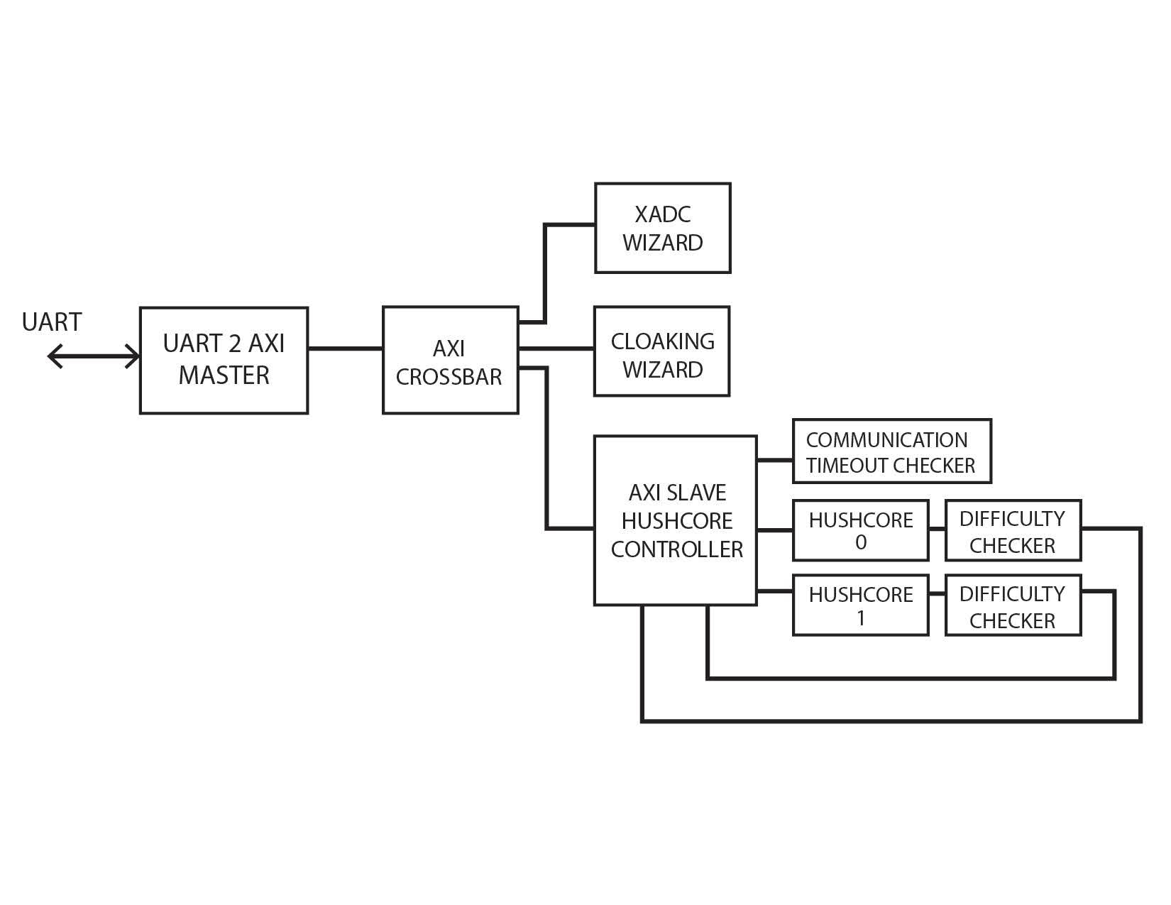
There were plenty of other small building blocks, but outside of the uart2axi master and the hash core itself, the other big one was the axiSlave interface, which acted as an addressable register interface to facilitate sending and collecting data from the other parts of the system that need it such as the hash state, the starting nonce, winning hashes, control signals, etc. The AXI slave interface is incredibly easy to use in SpinalHDL. It can be initiated with a single line. The code can be seen here.(TODO)
I also took advantage of some of the existing Xilinx IP blocks, most significantly the clocking wizard, XADC wizard, and AXI crossbar.
The hash core itself, a twist on the keccak cryptographic function, was adapted from an open-source VHDL implementation. The only non-Xilinx, open-source FPGA code I used for the project.
I used the GUI view in Vivado to hook up all the blocks, which can be seen here.

The hash cores take up the overwhelming majority of the resources and the Acorn is capable of fitting two hash cores in its logic at once. More could potentially fit in, but the thermal and power limits are already being stretched as it is.
A simplified block diagram is shown below.
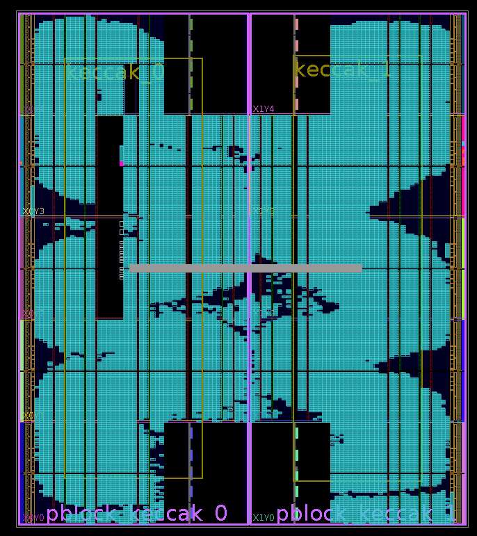
I also had to floorplan my design for the first time, which was an enlightening experience. Floorplanning enabled me to fit two hash cores, which was not possible without it. To do this, I set the Pblocks for each core to have half the FPGA for its constrains. The routed design can be seen below.
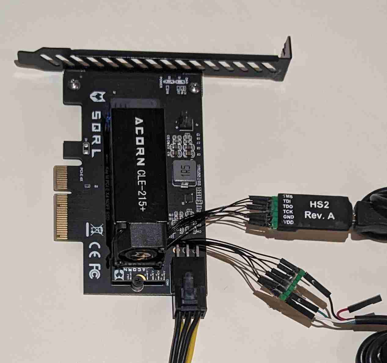
Connecting to the Acorn and powering it is also an annoying task as it’s designed for an M.2 motherboard slot, but I had more boards than motherboard slots. To do this, I took M.2 to PCIe adapters and mounted the acorns on there.
Some of the M.2 adapters had power ports, but others did not. So with the others I took old PCIe risers from the GPU mining days and mounted the board onto them.
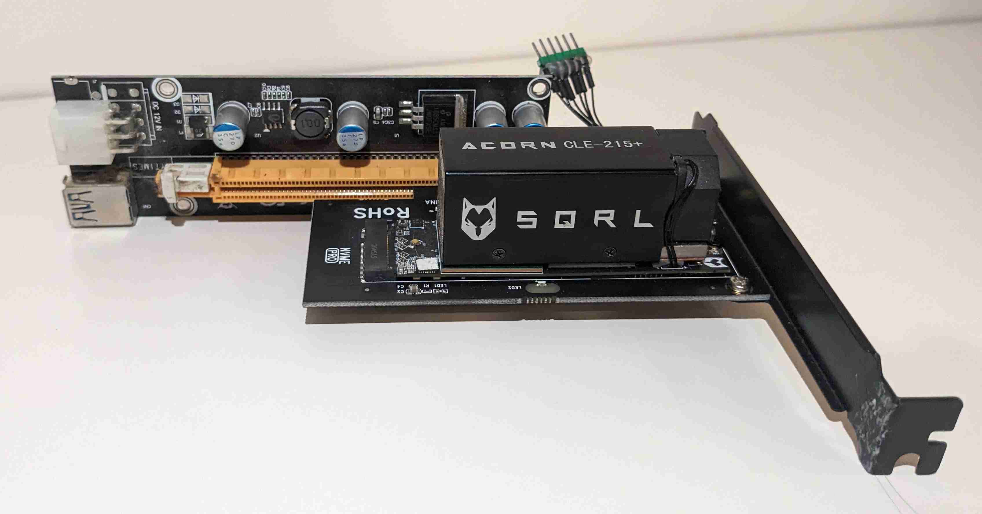
These provided the socket to allow a computer PSU to power the boards. Two levels of board adaptors, but it worked!
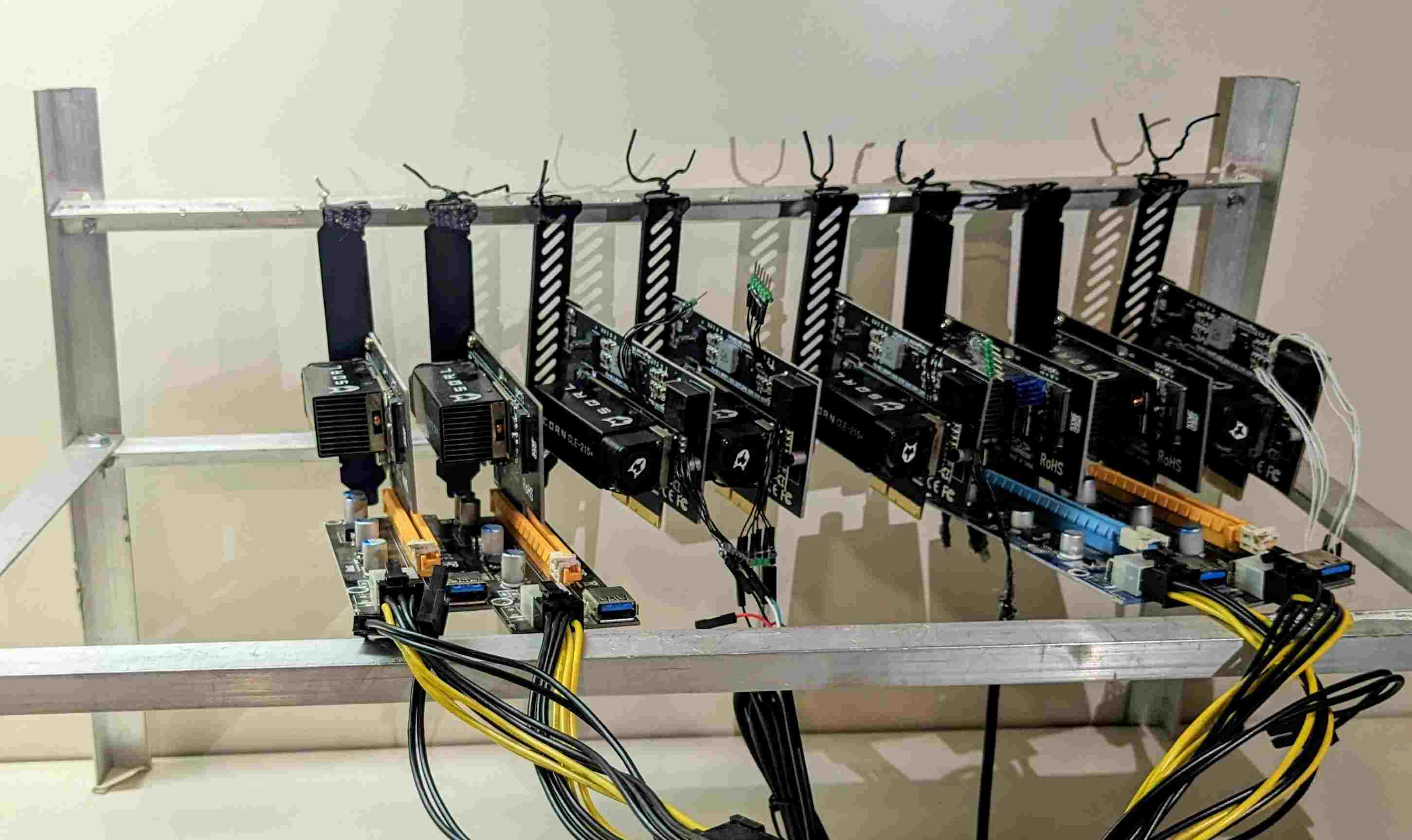
Below, you can see some of the boards mounted on a rack. Note these picture were taken after I moved and does not include all of the acorns or their proper hookups.
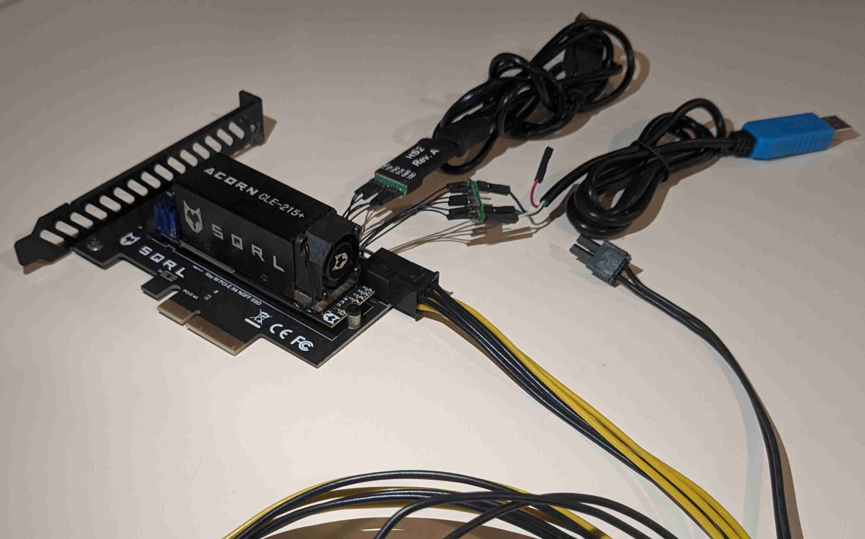
To facilitate communication with the FPGAs, I needed an alternative to buying a ridiculous amount of expensive debuggers. Cheap USB to UART devices can be found easily. The Acorn hardware is based on the Nitefury project. The schematic for the Nitefury shown here, reveals there are some pins exposed through a micro header and can be used for UART. So a cable (or 20) were soldered together from a cutting the pico connectors and soldering pin headers on. The image below shows the blue USB to UART dongle connected to the FPGA. Also note the second USB attachment also connected over the pico header is the debugger. Two adaptor cables were made per FPGA.
From here, with everything physically attached and the FPGA programmed, a host computer driver is needed.
The driver code is written in C which can be found here(TODO), as well as a standalone command line utility here(TODO).
The UART to AXI master is a memory-mapped io device; the master passes the data along to the slaves that reside at those addresses. The protocol to talk to a peripheral is as follows.
uint8_t cmd, // read or write
uint8_t seq, // sequence number
uint64_t address, // address
uint32_t data, // data
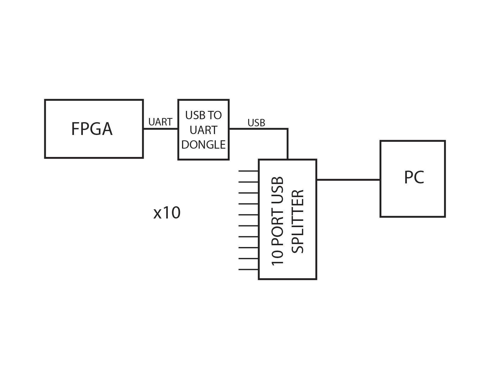
To facilitate 10 FPGAs at one time, a 10 port USB hub was used. A diagram of the connections from FPGA to PC is show below.
The cryptocurrency source code is written in Go and thus needs to compile the C code as well. Go has pretty good compatibility with C, so this is mostly a nonissue other than it is annoying. In the Go code, logic was added to coordinate the 10 FPGAs at once. The software abstraction levels can be seen below.
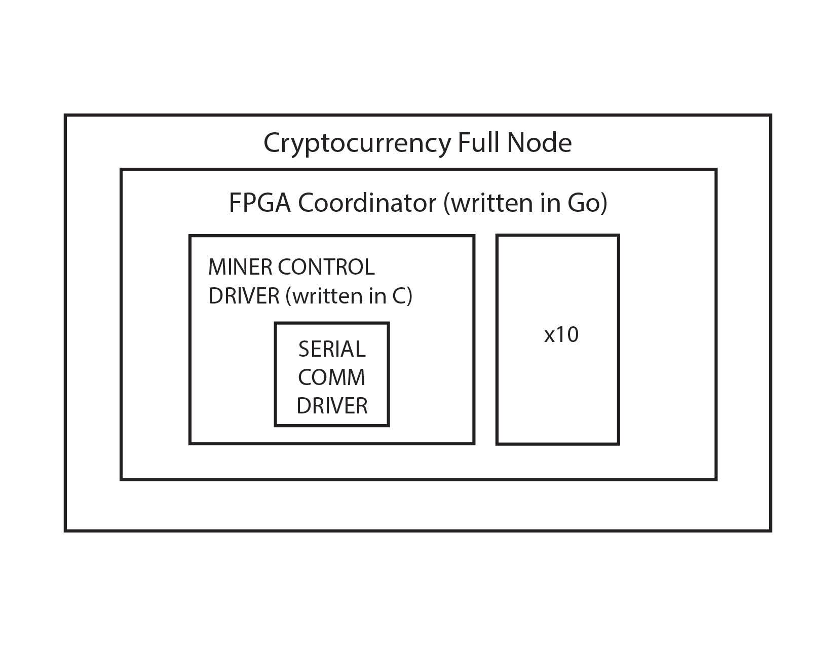
EXTRA FEATURES:
I added 3 extra features at this point that are huge quality-of-life improvements. The first and most important is that I added dynamic clock configuration to the hash core. This required handling clock-crossing domains as well but provided the ability to tune each board.
Next, I added a power saving feature that gave the FPGA itself the ability to idle the hash cores if no UART communication happened after 3 minutes.
Lastly, I added automatic shutdown if the PMIC temperature goes above the specified operating temperature range. The temperature is a known limiting factor in the system.
Unfortunately, after all this effort, I didn’t hit the predicted hashing speeds because of this Power Chip.
There were a few issues with it, most solvable, one not solvable.
ISSUES:
-
Due to a board layout design flaw, the temperature of the power chip could not be read as expected. I figured out a workaround for this by soldering different connections on the GPU riser breakout board. It’s a clever little trick to modify a cheap breakout board instead of the expensive FPGA board, if I do say so myself. In the end, the design flaw was such that half of a differential ADC was left floating, so I tied the PERST PCIe pin to the ground to give the differential ADC a stable reference. As PCIe was not used or hooked up in this setup, it posed no issues.
-
The thermal limits of the power chip were being reached even with the added PMIC heatsink. Several enhanced cooling options could solve this and have been looked into, such as water cooling or Peltier cooling.
-
(The real issue) - I ran up against the maximum power budget, so I could not push it any further. The chip was selected to meet the requirements of the m.2 specification, which specified a 15W maximum, even though the FPGA could pull way more. As this was not used in that M.2 configuration, the artificial power limit became the limitation. It’s a pretty big disappointment.
Unfortunately, with the thermal and power limits already being met, I am unable to run it at the capable clock speed. While the clock rate currently runs at 200 MHz, I predict that with sufficient power and heat dissipation, the clock rate could reach up to 400 MHz. But it’s not worth sacrificing a board trying to find out how far it can get in this setup. Additionally, another hash core could potentially fit as well. At the very least, a rolled hash core definitely could.
Naturally, as this is a small cryptocurrency, I didn’t get the luxury of mining pools. Typically, for mining, a simple connection to a pool provides only the exact hash block parameters necessary. Then, the host provides mining metrics and monitoring and payments proportional to the pooled hash rate. I instead had to integrate the FPGA into an entire blockchain node and coordinate 10 different FPGA boards, with 2 cores each.
TAKEAWAY:
In the end, this project was the culmination of hours upon hours of work, utilizing 6 different languages, various sophisticated software tools, and odd bits of hardware. Ultimately, I was able to create something from scratch that only a very select few in the community have been able to achieve, and I was the first to do it on Acorn FPGAs, breathing new life into them. And now, with the scaffolding in place, it shouldn’t be hard to port to other FPGAs or target other cryptocurrencies.

